Materials Characterization: Scanning Electron MicroscopyOne of the many instruments that uses electr
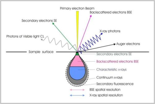
Materials Characterization: Scanning Electron MicroscopyOne of the many instruments that uses electrons to view the surface of a material is the scanning electron microscope, or SEM. In order to achieve a higher resolution and greater magnification than is possible with ordinary light, scientists turned to electrons and the resolution of an SEM can approach a few nanometers. SEMs don’t actually snap a picture of the surface but rather provide the contrast that produces an image. The resulting image, called a micrograph, is very similar to what you would expect if you could actually “see” the surface. SEM images are always monochrome but are often edited to produce false color images (sometimes similar to the real material, sometimes vastly different).How though, do electrons produce an image? It all depends on how they react with the sample. An SEM contains a series of magnetic lenses that focus the beam of electrons similarly to how glass lenses focus light in an optical microscope. This beam of electrons then hits the surface of the sample and can undergo either inelastic or elastic scattering, resulting in the emission of electrons. It is these emitted electrons that are analyzed. Secondary electrons are low-energy electrons that are ejected from the specimen atoms by inelastic scattering. Backscattered electrons are high-energy electrons from the original electron beam that are reflected or back-scattered by elastic scattering.Some of the most common methods for producing the electron beam itself are thermionic tungsten, LaB6, and hot and cold field emission.Unlike an optical microscope, an SEM has a few sample requirements. For one, the material has to be vacuum compatible. For another, it helps to have a conducting material. If your material isn’t a conductor it must be coated with a thin conducting film (usually around ten nanometers) of carbon, gold, or some other metal.Thanks to the fantastic images it can provide, the scanning electron microscope is one of the most widely used tools for materials characterization. Sources: ( 1 ) ( 2 ) ( 3 )Images: ( 1 ) ( 2 ) ( 3 ) ( 4 ) -- source link
Tumblr Blog : materialsscienceandengineering.tumblr.com
#materials science#science#electrons#mymsepost


